
PCB Layout of Chips On Board
Time:2022-06-27
Views:1841
The substrate is used as a carrier for silicon. The two main reasons are to avoid CTE mismatch and to protect integrated circuits from environmental impacts.
Another advantage is that it can be dispersed and connected, allowing for the use of lower tech PCBs. The delivery time for certain types of packaging is measured
in months. They also spent a lot of money on non recurring engineering (NRE), and each item requires a little more. In some cases, it is more meaningful to discard
the adapter and place the device directly on the PCB. Let‘s take a look at this idea.
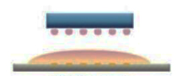
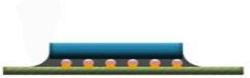
Chip On Board (COB) is what it says on tin cans. There are basically two methods for performing chip mounting. One method is to set a convex block at the bottom
of the tube core; Just like a regular BGA, but smaller. These ‘flip chip‘ will test your PCB supplier‘s ability to create micro packages. Then they will test your assembly
partner‘s ability to place, reflow, and flip chip (FCOB) on the bottom filler board.

Fluxing
die placement
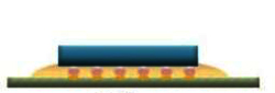
reflow

Flux cleaning
underfil
cure
of the tube core; Just like a regular BGA, but smaller. These ‘flip chip‘ will test your PCB supplier‘s ability to create micro packages. Then they will test your assembly
partner‘s ability to place, reflow, and flip chip (FCOB) on the bottom filler board.
Fluxing
die placement
reflow
Flux cleaning
underfil
cure
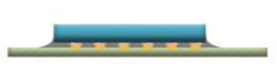
Due to the different thermal expansion coefficients of materials, bottom filling is necessary. If there is no bottom filling, CTE mismatch will exert pressure on the flip chip,
reaching the level of unreliable connection.
reaching the level of unreliable connection.